

cmos运算放大器设计
摘 要 :集成运算放大器是一种重要的电子元件,它的主要作用是提供足够的增益。结合外加的反馈电路,运算放大器可实现对模拟信号的多种处理功能,比如放大、微分、积分、求和、对数等运算。理想的放大器应该无噪声、具有无穷大增益和输入阻抗、无穷小输出阻抗以及零失调电压等。这篇论文主要研究了运算放大器电路的基本工作原理和对它的版图设计。运算放大器电路主要包括五个部分:差分跨导,高增益级,输出缓冲,偏置电路和补偿电路,差分跨导级构成运放的输入级,有时还起从双端差分输入到单端输出的变换作用。通常,整个电路的增益,一大部分是由输入差分级提供的,反相器一般会作为第二级。当差分输入级没有完成差分-单端变换时,就由第二级反相器来完成。版图设计,又称物理设计,是电路设计工程师交给工艺工程师的集成电路制造蓝图。
关键词:放大器;电路;版图;工艺
Subject: Integrated operational amplifier is a kind of important electronic components, its main function is to provide enough gain. In combination with additional feedback circuit, operational amplifier can be realized on a variety of processing capabilities of analog signals, such as amplification, differential, integral, summation and logarithmic computation. No noise, the ideal amplifier should have infinite gain and input impedance, output impedance of infinitesimal and zero offset voltage, etc. This paper mainly studies the basic working principle of the operational amplifier circuit and layout design of it. Operational amplifier circuit mainly includes five parts: the difference transconductance, high gain, output buffer, the bias circuit and compensation circuit, differential levels transconductance constitute the op-amp input, sometimes up from the double differential input to output single-ended conversion function. Usually, the gain of the whole circuit, a mostly provided by the input differential classification and inverter are generally as the second level. When the differential input stage didn't finish the difference - single-ended conversion, are done by the second inverter. Landscape design, also known as physical design, circuit design engineer is to the integrated circuit manufacturing blueprint of process engineer.
Keywords: Amplifier; Circuit; Layout; Process
目录
第一章 绪论 1
1.1集成电路的发明与发展 1
1.2 MOS管的历史 2
1.3 本文的主要研究内容 3
第二章 CMOS运算放大器电路的理论知识 3
2.1 集成电路的设计流程 3
2.2 集成运放电路的组成及各部分的作用 4
2.2.1 集成运放电路的设计流程 4
2.2.2 CMOS集成运放电路的组成部分 5
2.2.3两级运算放大器原理简单分析 5
2.3 StartupCmp的原理分析 5
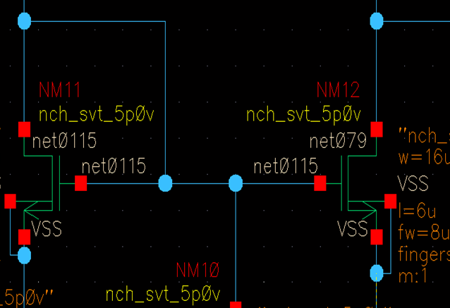
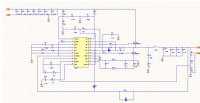
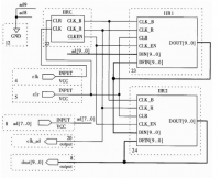
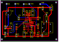
第三章 CMOS运算放大器的版图设计 8
3.1 版图的设计规则 8
3.1.1 硅栅CMOS工艺版图和工艺的关系 8
3.1.2版图设计规则 8
3.1.3版图的基本规则 12
3.1.4注意器件的匹配: 15
3.2 版图设计 16
3.2.1各个基本器件的版图 16
3.2.2 局部版图设计 18
3.3 整体版图 24
3.3.1 布局 25
3.3.2 布线 26
3.4 CMOS运算放大器版图验证 26
3.4.1 DRC验证 26
3.4.2 LVS验证 28
3.4.3版图的整体检查 30
3.4.4完成版图 31
3.5 cadence软件的使用 31
第四章 总结与展望 38
小结与致谢 38
参考文献 40
参考文献
[1] 刘树林,程红丽.低频电子线路.北京:机械工业出版社.2007.8
[2] 朱正涌,张海洋,朱元红.半导体集成电路(第二版).北京:清华大学出版社.2009.4 [3] 刘树林,[3]张华曹,柴长春.半导体器件物理.北京:电子工业出版社.2005.2
[4] 关旭东.硅集成电路工艺基础.北京:北京大学出版社.2003.12
[5] (美)Behzad Razavi.模拟CMOS集成电路设计.西安:西安交通大学出版社.2010.3
[6] 张建人. MOS集成电路分析与设计基础.北京:电子工业出版社.
[7] (美)Alan Hast:电子工业出版社.
[8] 张延庆,张开华,朱兆宗.半导体集成电路.上海:上海科学技术学院
[9] 王振红.运算放大器应用.北京:化学工业出版社.2009.4
[10] 谭博学,苗汇静.集成电路原理及应用. 北京:电子工业出版社.
[11] 李联.MOS运算放大器―原理、设计与应用.上海:复旦大学出版社
[12] 吴建辉.CMOS模拟集成电路分析与设计.北京:电子工业出版社.2011.5
[13] 李伟华.集成电路版图基础.北京:清华大学出版社.2006.1
[14]曾庆贵,姜玉稀.集成电路版图设计教程.北京:上海科学技术出版社.2012.3
http://www.bysj1.com/html/5839.html
http://www.bysj1.com/html/6302.html