


CIGS薄膜太阳能电池的设计.
摘 要: 首先介绍了铜铟镓硒(CIGS)薄膜太阳能电池原理以及目前在研究和生产过程中电池的制备方法和工艺,重点介绍了两种高效率制备薄膜的工艺,最后阐述了铜铟镓硒(CIGS)太阳能电池的应用情况,并展望了铜铟镓硒(CIGS)发展趋势。
关键词:CIGS;薄膜;太阳能电池
毕业设计说明书目录
1 引言………………………………………………………………………………………13
2 原理………………………………………………………………………………………14
2.1太阳能电池的定义………………………………………………………………14
2.2太阳能电池的工作原理…………………………………………………………14
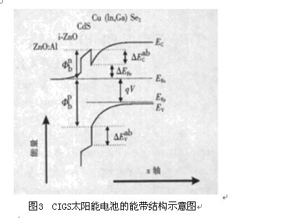
2. 3 CIGS薄膜太阳能电池的工作原理………………………………………………15
3 电池的制备………………………………………………………………………………15
3.1 CIGS薄膜太阳能电池的构成……………………………………………………15
3.2 衬底材料的制备…………………………………………………………………16
3. 3 背电极Mo 的制备………………………………………………………………17
3. 4 电池吸收层CIGS薄膜的制备…………………………………………………17
3. 5 电池缓冲层CdS的制备…………………………………………………………17
3. 6窗口层ZnO薄膜的制备…………………………………………………………18
4 生产工艺…………………………………………………………………………………18
4.1 CIS和CIGS材料特性…………………………………………………………18
4.2 CIGS吸收层制备工艺…………………………………………………………19
4.3共蒸发法和后硒化法……………………………………………………………23
4.4电池缓冲层的制备工艺…………………………………………………………25
4.5窗口层ZnO薄膜的制备工艺 …………………………………………………26
5 应用设计…………………………………………………………………………………26
5. 1光伏系统原理与应用……………………………………………………………27
5. 2光伏建筑一体化的概念与分类…………………………………………………28
5. 3光伏建筑一体化(BIPV)对光伏方阵与光伏组件的要求……………………28
5. 4光伏建筑一体化BIPV的设计…………………………………………………29
5. 5 太阳能光伏建筑一体化的优势…………………………………………………30
5. 6 CIGS薄膜太阳能电池产业化应用前景………………………………………30
参考文献
[1] CHOPRA K L,PAULSON P D,DUTTA V. Thin film solar cell: an overview[J]. Progress in Photovoltaics: Research and Applicati-ons,2004,12: 69~92.
[2] 刘玉萍,陈枫,郭爱波等. AZO透明导电薄膜的制备技术及应用进展[J].与低温,2007, 13 ( 1):1~5.
[3] Jonas Hodstrom,Marika Bodegard,Dimitri Hariskoas,et al .ZnO/ CdS/ Cu( In ,Ga) Se2,thin film solar cells with improvedperformance. Schwartz R J . The 23rd IEEE Photovoltaic Spe -cialists Conferencc ,Louisville KY,1993[C] . Louisville,KY:Electron Device Society,1993 :364— 3711.
[4] 李长健,王俊清等. CIS/CdS薄膜太阳电池工艺探讨.南开大学学报(自然科学版),1998,31(4) :95— 100.
[5] Y amada A,Matsubara K,Sakurai K,et al . E ffect of bandoffset on the open circuit v oltage of heterojunction CuIn1-xGaxSe2 s olar cells [J ] . Applied Physics Letters,2004,85 :5607— 5609.
[6] Rau U,Schock HW. Electronic properties of Cu( In ,Ga) Se2heterojunction s olar cells -recent achievements , current under-standing,and future changes[J ] . Applied Physics A , 1999,69 : 131— 147.
[7] Yuming Xue,Sun Yun,Piao Y ingmei,et al . The depositionof two kinds of CdS thin films with di fferent crystal phases andtheir in fluences on Cu ( In ,G a) Se2 thin film s olar cells[A] .19th European Photov oltaic S olar Energy Con ference [ C ] ,Paris , France,2004 : 1843— 1846.
[8] 陈光华,邓金祥. 新型电子薄膜材料[M] . 北京:化学工业出版社,0032.
[9] White F R,Clak A H,Gxaf M C. Molecular beam epitaxytechniques for preparing CuInSe2 thin films[J ] . Appl Phys ,1979,50 : 544.
[10] Kaelin M,Rudmann D,Kurdesau F,et al. CIS and layers f rom selenized nanoparticle precursors[J ] . Thin SolidFilms,2003,4312432 :58.
[11] Eberspacher C,Paula K,Serra J . Non-vacuum processing of solar cells [ A ] . Photovoltaic Specialist s Conference,2002. Conference Records of the 29th IEEE PVSEC [C] . USA : New Orleans,2002. 684.
[12] Kaelin M,Rudamann D,Kurdesau F,et al. Low-cost solar cells by paste coating and selenization [J ] . Thin Solid Films,2004 , 457 :391.
[13] Femandez A M,Bhattacharya R N. Elect rodeposition of CuIn1 - x Ga x Se2 precursor films :optimization of film composition and morphology[J ] . Thin Solid Films,2005 , 474 :10.
[14] Ganchev M,Kois J,Kaelin M,et al. Preparation of Cu ( In ,Ga) Se2 layers by selenization of elect rodeposited Cu2In2Ga precursors[J ] . Thin Solid Films , 2006, 5112512 :325.
[15] GABOR M,JOHN R,TUTTLE, DAVID S. Albin, High-efficiency CuInxGa1–xSe2 solar cells made from (Inx,Ga1–x)2Se3 precursor films[J]. Appl Phys,1994,65: 198-200.
[16] NIKI S,FONS P J, YAMADA A. Effects of the surface Cu2-xSe phase on the growth and properties of CuInSe2 films[J]. Applied Physics Letters,1999,74: 1630-1633.
[17] LUNDBERG O,EDOFF M,STOLT L. The effect of Ga-grading in CIGS thin film solar cells Thin Solid Films[J]. 2004,1: 480-481.
[18] Gao X D,L iXM,YuW D. Mor phol ogy and op tical p r oper-ties of amor phous ZnS fil ms deposited by ultrasonic- assistedsuccessive i onic layer ads or p ti on and reacti on method [ J ].Thin Solid Fil ms,2004,468: 432 47.
[19] 马 锦,马云芳,宋学萍,孙兆奇.厚度对 ZnS薄膜结构和应力的影响 [ J ]. 合肥工业大学学报 (自然科学版 ),2007,30: 72 10.
[20] Nakada T,MizutaniM. High- effciency Cu ( In, Ga) Se2 thin-fil m solar cells with a CBD- ZnS buffer layer Solar Energy[ J ]. Materials and Solar Cells,2001,67: 2552 260.
[21] ContrerasM A,Nakada T, HongoM, et al . ZnO / ZnS (O ,OH) / Cu ( In , Ga) Se2 / Mo s olar cell with 18. 6% effi-ciency . Proceeding 3 rd World Conference of Phot ovoltaicEnergy Conversi on [C ]. Osaka, Japan,2003 : 216.