

二进制硬件乘法器的FPGA实现设计
摘 要
乘法器是处理器进行科学计算和数字信号处理的基本硬件结构,是现代微处理器中的重要部件。乘法器完成一次乘法操作的周期基本上决定了微处理器的主频。本文基于FPGA,采用VHDL语言,结合MAX+plusⅡ这个强大的软件平台设计了8位二进制乘法器,并对其进行符号扩展,使其可以统一处理8位带符号数和无符号数。
高速乘法器设计通常分为三个关键步骤:部分积产生、部分积累加和最终结果获得。本文对部分积产生过程采用改进多算法,有效减少部分积加法项;为了统一带符号和无符号数,对部分积进行符号扩展;而对部分积的累加则采取3-2压缩器和4-2压缩器进行压缩;最终结果的获得则以一个根据部分积累加结果到达时间的不同进行延迟优化的选择进位加法器将累加结果和累加进位相加而得。
关键词:乘法器 改进多算法 压缩器 选择进位加法器
Abstract: The multiplier is not only the basic hardware structure of the processor for scientific computing and digital signal processing but also an important component of modern microprocessors. This design for 8-bit binary multiplier is based on FPGA, using VHDL language, and proved by the MAX+plusⅡ software platform. The multiplicand has an extended sign bit so that the multiplier can unify 8-bit signed and unsigned.
High-speed multiplier design is usually divided into three key steps: partial product generation circuit, accumulator and adder. In this paper, the partial product generation process uses the modified Booth algorithm, so that the partial product addition terms can be effectively reduced. The accumulation of partial products takes 3-2 compressor and 4-2 compressor to compress. The final result is obtained with select carry adder.
Key words: multiplier the modified Booth algorithm compressor select carry adder
摘 要 I
引言 3
1 设计任务及设计要求 3
1.1 设计任务 3
1.2 设计要求 4
1.3 编码器的真值表 4
2 设计总体思路 4
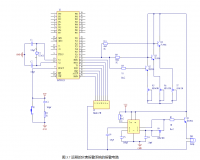
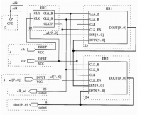
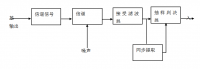
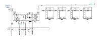
2.1 系统框图 4
2.2 各单元电路设计 5
2.2.1 输入模块 5
2.2.2 数字与符号分离模块 5
2.2.3 乘法运算模块 6
2.2.4 数字与符号组合模块 6
2.2.5 显示控制模块 6
2.2.6 输出数字与符号分离模块 7
2.2.7 进制转换模块 7
2.2.8 消零模块 8
2.2.9 seltime模块 8
2.2.10 led模块 9
2.2.11 灭点模块 9
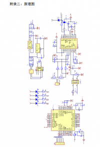
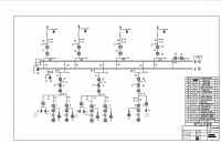
2.3 总电路图设计 9
3 理论分析及设计 10
3.1 乘法器的数据格式 10
3.1.1 二进制的表示 10
3.1.2 无符号数的运算 10
3.1.3 带符号数的运算 10
3.1.4 带符号数的符号扩展表示 11
3.2 乘法器算法 11
3.2.1 移位相加算法 11
3.2.2 Booth算法 12
3.2.3 改进型Booth算法 13
3.3 加法器 17
3.3.1 半加器 17
3.3.2 全加器 17
3.3.3 串行进位加法器 18
3.3.4 超前进位加法器 19
3.3.5 选择进位加法器 20
3.4 压缩器 21
4 设计改进及总结 24
4.1 设计改进 24
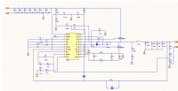
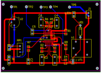
4.1.1 电路图: 24
4.1.2 INPUT模块 24
4.1.3 SEGSEL模块 26
4.1.4 DELED模块 27
4.1.5 电路图 28
4.1.6 仿真波形图 29
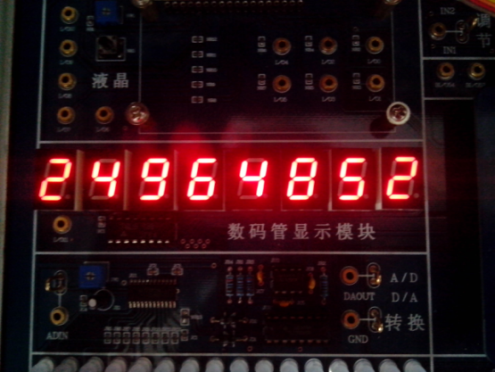
4.1.7 实验箱调试 29
4.2 设计总结 30
参考文献 30
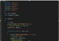
附录:程序部分 31
1 输入模块 31
2 数字与符号分离模块 32
3 乘法运算模块 32
4 数字与符号组合模块 33
5 显示控制模块 33
6 输出数字与符号分离模块 34
7 进制转换模块 35
8 消零模块 36
9 seltime模块 37
10 led模块 38
参考文献
[1] 黄任.VHDL入门·解惑·经典实例·经验总结.北京:北京航空航天大学出版社,2005.
[2] 黄仁欣.EDA技术实用教程.北京:清华大学出版社,2006.
[3] 潘松,黄继业.EDA技术实用教程.北京:科学出版社,2005.
http://www.bysj1.com/ http://www.bysj1.com/html/5215.html http://www.bysj1.com